| ||
| ||
| ||
| ||
| ||
|
strchan Paper
Description: OpenSS7 Online Papers
A PDF version of this document is available here.
High Density SONET/SDH MG Interface for VoIP Trunking
White Paper
Abstract:
Background
Interworking of voice over IP to PSTN trunking has traditionally used a decomposed architecture of Media Gateway (MG) and Media Gateway Controller (MGC or SoftSwitch). Media Gateways (MG) have been typically designed using Time Division Multiplexing (TDM) components and principles suitable for the Public Switched Telephone Network (PSTN). This use of hard real-time TDM components in access card and voice processing designs has led to reduced scalability through the inappropriate application of PSTN TDM principles to VoIP trunking designs.
For example, the application of H.110 TDM busses and DSP resources in card and system designs has increased the cost of MG subsystems as well as reducing scalability, increasing vendor lock-in, and dedicating special purpose hardware where low-cost scalable commodity host processing power would more than suffice.
Maximization of commodity host processor utilization and software approaches2 leads to greatly reduced interface card per-channel costs as well as providing for greater densities and scalability, and removing vendor lock-in with a Commodity Off-The Shelf (COTS) solution.
Table 1 lists the various costs of legacy solutions
in comparison to the current design.
The analysis provides the per-channel cost of various interface solutions considering only the cost of interface equipment (and not the cost of the host processors). As can be seen from Table 1, the cost per channel of legacy approaches range from about $1.25 per channel to $5.65 per channel just for interface cards, whereas the SONET/SDH design presented in this paper provides for a cost of $0.03 per channel: a dramatic decrease.
Tormenta Lessons
In general the low-density quad E1/T1/J1 Tormenta II and III cards were quite successfully and are still widely manufactured and used. When the Tormenta II card was originally designed (2000, 2001 and 2002) the host equipment that could house such a card were based on 32-bit 33 MHz PCI designs that could not sustain full bus rate burst speeds. This PCI design replaced the Tormenta I cards which was an ISA card. The ISA bus could not sustain a transfer rate that would permit more than 2 T1s to be provided on the same card. Competing proprietary designs at the time (such as that provided by Pika) ran to $5000 per card for a single T1, or over $50.00 per channel.
The Tormenta II and III card design is illustrated in Figure 1.
The card consists of: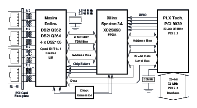
- Line interface transformers and connectors. LIU transformers and RJ-45 PCI card faceplate connectors for interfacing 4 E1/T1/J1 lines. (100 Ohm balanced for T1 or J1 and 120 Ohm balanced for E1.)
- Framer and LIU. Integrated quad E1/T1/J1 framers and line interface units (Maxim Dallas DS21Q352 (T1), DS21Q354 (E1) for Tormenta II; or DS2155 (E1/T1/J1) for Tormenta III).
- Field Programmable Gate Array. The Xilinx Spartan 3A XC2S50 5C Field Programmable Gate Array (FPGA) primarily provides buffering between the 8.192 MHz byte-interleaved TDM bus and the PCI Interface.
- PCI Interface. The PLX Technology PCI 9030 interface chip is a slave 32-bit 33 MHz PCI target. This chip provides host processor access to FPGA buffered E1, T1 or J1 frames.
The success (both engineering and economic) of the cards has taught several lessons:
- Reduce hardware functions. This increases the longevity of the card. Functions performed by specialized hardware should require hardware solutions due to real-time constraints (e.g. framers and line interface units).
- Keep the design open and free. This permits improvements in the design or implementation to be widely adopted. It also permits a shared learning curve, promotes competitive pricing, and avoids vendor lock-in.
- Move data to the host processor early. Once section timing, framing and overheads have been processed, the data payloads should be moved to the host processor for processing.
- Use host processor for scale. Permits these functions to be performed where performance in the industry is scaling the fastest: commodity processors.
Application of these principles has led to a SONET/SDH design where synchronous payload extraction and tributary alignment is performing using a SONET/SDH framer device, but payload processing has been moved to the commodity host processor by passing VC payload directly to and from host memory using PCI bus mastering.
Application to MG and VoIP Trunking
Normally, TDM systems are hard real-time systems where processing is performed primarily in specialized hardware and supervisory and control functions are performed using software and more general purpose processors. This results in latency of voice samples through a system being significantly less than 1 millisecond (typically 125 microseconds).
Media Gateways and VoIP Trunking, on the other hand, have significant latencies. Therefore, hard real-time specialized hardware approaches are inefficient for MG and VoIP trunking designs. Hardware designed to perform operations within 125 microseconds (e.g. DSP, TDM bus and switching chips) are inappropriate considering the packetization delay of an RTP G.711 encoded packet is 30 milliseconds (or 2 orders of magnitude greater) and echo cancellation algorithms use a 120 millisecond tail (or 3 orders of magnitude greater).
By avoiding use of these high-cost components to perform TDM processing within 125 microseconds, the cost of interface equipment can be significantly reduced. Criteria for functional placement are as follows:
- Is hard real-time response absolutely required by the function? For VoIP, the answer to this question for all processing of the voice samples is no. DSP (Digital Signal Processors), and TDM (Time Division Multiplexing) bus hardware, are an emphatic no.
- Can the function be performed using software and memory? This includes all voice sample processing which can easily be performed in host memory with general purpose processors and software.
- Can the function be performed more efficiently by waiting and block processing? For VoIP, this answer is yes for all voice sample processing. This includes codecs, echo cancellation, transcoding, tone detection and tone generation.
- Must the data be examined by, or otherwise transferred to, the host? For VoIP this answer becomes yes: all data must pass through a host processor anyway.
SONET/SDH Card Design
Figure 2 illustrates the overall SONET/SDH line card design, with a x4-lane PCIe option shown in grey.
This design bears significant resemblance to the Tormenta II and III card designs. The guiding principles for the SONET/SDH design are: move data to the host as early as possible; avoid external TDM bus interfaces; and, avoid performing functions in specialized hardware. The SONET/SDH OC-48 interface card design consists of the same types of integrated components: Optical Interface, SONET/SDH Framer, FPGA, PCI Interface, and optional PCIe bridge.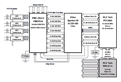
The estimated costs of the primary components on the card, and representative
pluggable optical transceiver costs are listed in Table
2.
The design satisfies the objective of having a full SONET/SDH interface card with a cost less than $1,000.00 per card.3
Optical Transceivers
The SFP (Small Form-Factor Pluggable) transceivers are illustrated in Figure 3.
The optical interface consists of 4 Small Form-Factor (SFP) receptacles for SPF optical (OC-3/12/48) or electrical (STS-3e/STM-1e 75 Ohm coaxial mini-BNC) tranceivers. These accept hot-pluggable transceivers. For the card's application (which is primarly short-reach interface to a SONET/SDH ADM or DCCS), only short reach (SX) modules are necessary; however, the pluggable tranceiver modules permit a range of reaches. The optical or electrical transceivers can be any combination of same speed tranceivers with a total aggregate 1+1 protected or unprotected OC-48 line rate. That is, the 4 SFP SX transceivers can be one of: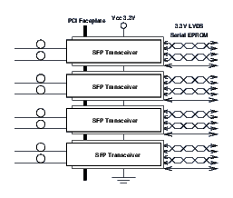
- 1 to 2 x OC-48. One or two (1+1 APS) 2488 MHz (OC-48) SFP optical transceivers: duplex SMF optical transceivers with 0-10 km reach.
- 1 to 4 x OC-12. Up to 4 622 MHz SFP SX optical transceivers in unprotected or 1+1 APS configuration: duplex SMF optical transceivers.
- 1 to 4 x EC-3/OC-3. Up to 4 155 MHz SFP SX electrical or optical transceivers in unprotected or 1+1 APS configuration: bidirectional MMF or duplex SMF optical transceivers or duplex 75 Ohm electrical transceivers.
SONET/SDH Framer
The SONET/SDH framer is illustrated in Figure 4.
The SONET/SDH Framer and LIU can support 1+1 OC-48 interfaces, 4 x OC-12 interfaces, 4 x OC-3/EC-3 interfaces. The SONET/SDH framers can support a maximum (fully 1+1 protected) capacity of 32,256 voice channels. The minimum capacity is one VT1.5/TU11 or 24 channels. The interface scales from 1.536 kbps to 2.064384 Gbps. The SONET/SDH Framer supports an internal telecom bus that is a 77.76 MHz 32-bit or 4x8-bit parallel data interface bus that is used to clock VC-3, VC-4, VC-4-4c frames between the SONET/SDH chip and the FPGA.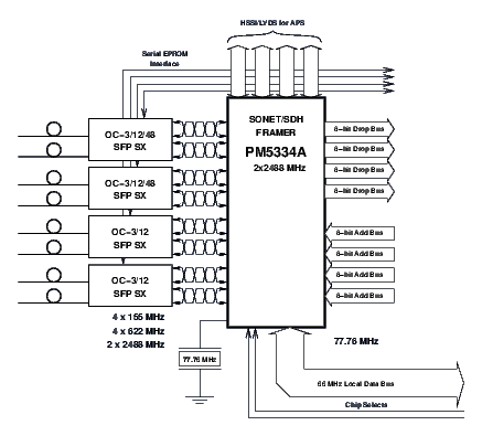
The SONET/SDH framer chip selected is the PMC Sierra PM5334A chip. This is a 2x2488 (1+1 OC-48) SONET/SDH framer and TU3 mapper. At the time of writing, this chip had a cost of approximately $315.00 USD in low volumes.5
Field Programmable Gate Array
The Field Programmable Gate Array (FPGA) is illustrated in Figure 5.
A FPGA is used to tranlsate between the internal 77.76 MHz parallel telecom bus provided by the SONET/SDH framer chip and internal FIFOs used for dynamic DMA bus mastered transfers between the card and the host. One of the most significant costs in FPGA chips is the amount of on-chip RAM banks that are available. Extensive use of on-chip RAM significantly increases the cost of the chip.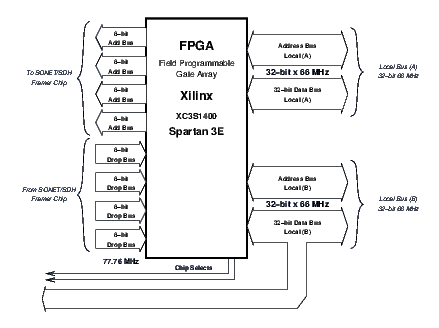
Therefore, this design, rather than internally buffering 1ms of channel data (as does the Spartan 3A XC2S50 in the Tormenta II design), relies on the ability of the PCI interface chip to perform bus mastered DMA burst transfers to host memory. A far reduced amount of on-chip RAM is required and is only used in a FIFO arrangement to buffer burst transfers to and from the PCI bus. Payload self-synchronizing scrambling/descrambling may also performed in the FPGA.
A valueable characteristic of modern FPGAs is the ability to use readily available low-cost or free tools and open-source VDHL and synthesis to permit design changes increasing the openness of the card design.
The FPGA chip selected is the Xilinx Spartan 3A Extended XC3S1400A-FG484-5C chip. At the time of writing, this chip had a cost of approximately $73.00 USD per device in low volumes.6
PCI Interface
The PCI Interface is illustrated in Figure 6.
A 64-bit 66MHz PCI interface is used to interface the card either directly to the host, or optionally to a 4-lane PCI Express bridge to the host processor. The PCI interface is capable of scatter/gather dynamic bus mastered DMA with descriptor rings (in a similar fashion to many Ethernet or ATM interface card designs). This permits a maximum burst transfer rate of 4.224 Gbps which is close to the full channel capacity of the OC-48 interface which is 4.129 Gbps. An optional x4-lane PCI Express bridge (8 Gbps) provides PCI express interface with an additional 10K buffering and read-ahead capability.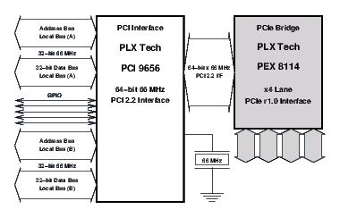
The interface can also operate at 32-bit 33MHz (or optionally into 1-lane PCI Express) and in this mode is capable of transfering the full channel capacity of an OC-12 interface or 8064 channels. The PCI 2.2 interface is capable of 3.3V or 5.0V operation.
This PCI interface design choice permits either a PCI card to be used in PCI-X riser in popular 1U and 2U server chasses. Use of a traditional PCI interface permits reuse of existing server equipment. Optional PCIe interface supports use in newer generation server equipment only providing PCIe card expansion.
The PCI interface chips selected are the PLX Technology, Inc. PCI 9656-BA66BIG chip, and optional PEX 8114 chip. At the time of writing, each of these chips had a cost of approximately $45.00 USD in low volumes.7
Software
Software for the SONET/SDH interface card can utilize OpenSS7 open-source software. Software consists of a multiplex (MX) driver, RTP driver and media gateway (MG) multiplexing driver as illustrated in Figure 7.
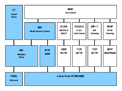
The Multiplex (MX) driver is a device driver designed specifically for use with the SONET/SDH card, but utilizes an interface (MXI) that is common to all PDH drivers. The driver performs low-order path processing, VC mapping, VT/TU overhead processing and TU-3/VC-3 framing. Tributaries are demultiplexed into primary VT1.5/TU11 or VT2/TU12 streams that are linked beneath the Media Gateway (MG) multiplexing pseudo-device driver.
RTP streams are managed by the RTP driver which is also linked beneath the MG multiplexing driver.
The Media Gateway (MG) multiplexing driver performs media gateway functions subject to either local control or external H.248 connection. This permits either stand-alone MG operation or integrated MG/MGC operation. The MG driver performs interconnection between the VT channels of the MX driver and the RTP streams of the RTP driver and performs transcoding, echo cancellation and T.38 Fax processing.
A Zaptel8 (ZT) driver can be provided for transparent support of IAX, Asterisk, FreeSwitch and other Zaptel/IAX supporting soft real-time applications.
In general, because SPE and payload are processed in the host, it is possible to develop drivers for ATM (AAL1, AAL2, AAL5), PoS, and other SONET/SDH layer 2 protocols without alterations to the interface card design.
Host Considerations
Typically the primary factors driving Host selection (for housing the interface cards and providing Host compute power for performing voice processing functions) are environmental in nature.
When the Host is to be installed in a Central Office environment, NEBS and ETSI conformance, such as DC power and local alarm display, is necessary. When the host is to be installed in a data center, NEBS and ETSI compliance is too honerous and a reduced cost host can be selected that meets the environmental considerations of the data center. Carrier grade hosts currently include the NEBS/ETSI certified IBM x3650T 2U chassis (based on the Intel/Kontron TIGI2U design) or the NEBS/ETSI compliant Kontron TIGW1U (based on the Intel TIGW1U design).
In general, however, any Host that meets the needs of the target environment is suitable for the OC-48 card design.
Back-End Connectivity
The larger scale of the SONET/SDH OC-48 interface card design challenges the back-end connectivity of the Host. Channelized OC-48 provides 2.064 Gbps duplex (4.129 Gpbs) G.711 voice samples. With an overhead of 20% for RTP headers (G.711 30ms coded voice), this requires Ethernet connectivity with 4.955 Gbps link capacity. This requires quad GigE interfaces. Hosts (such as the x3650T) that provide dual GigE interfaces must be equipped with additional GigE ports (or upgraded to 10G or 20G links) for back-end network connectivity to be able to process the full capacity of a single OC-48 (or quad OC-12) interface card.
Example Applications
Following are two application examples for very high density VoIP trunking.
1U Enterprise Application
A typical 1U Enterprise application utilizes commodity 1U servers (e.g. such as the 1U HP Proliant DL360 G6 server (DL308a) or 2U HP Proliant DL380 G6 server (DL308b)). The application may provide 1 x OC-48 (unprotected or 1+1 APS) or 4 x OC-12 (unprotected or 1+1 APS) connections processing VoIP trunking into 4 GigE rails. The maximum processing capacity is 32,256 channels. System hardware cost is approximately $6,000 providing for a CAPEX of $0.15 per channel. CAPEX can be further reduced by retargeting existing or decommissioned high power consumption commodity 1U servers.
1U ITSP Application
A typical 1U Internet Telephony Service Provider application utilizes the Kontron TIGW1U NEBS/ETSI compliant server or equivalent. The application provides 1 x OC-48 (1+1 APS) connections processing VoIP trunking into 4 GigE rails. The maximum processing capacity is 32,256 protection switched channels. System hardware cost is approximately $8,000 providing for a CAPEX of $0.25 per channel.
2U Carrier Application
Figure 8 illustrates a 2U Carrier grade application using the IBM x3650T NEBS/ETSI certified (or Intel/Kontron TIGI2U or Kontron TIGH2U) server.
Other options include the NEBS/ETSI certified HP Proliant DL385 G5 CG server.(DL308c) The application provides 4 x 2 (1+1 APS) OC-12 connections and 4 x OC-3 connections processing VoIP trunking into 6 GigE rails. The maximum processing capacity is 40,320 protection switched channels. System hardware cost is approximately $15,000 for a CAPEX of $0.37 per channel.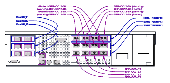
The application consists of:
- Three SONET/SDH Full-Height, Half-Length PCI cards running at 3.3V, 64-bits, 66 MHz, BDM.
- Two sets of four SFP-OC12-SX duplex single-mode fiber small form-factor pluggable transceivers. Each of two SONET/SDH cards has 2 working and 2 protect OC-12 interfaces.
- One set of four SFP-OC3-SX bidirectional single-mode fiber small form-factor pluggable transceivers. One SONET/SDH card houses all four OC-3 interfaces.
- Dual GigE rails (onboard).
- Three dual GigE half-height, half-length PCIe four-lane cards.
Summary and Conclusions
With the application of criteria suited for a high-density VoIP trunking application, it is possible to significantly reduce the cost per channel of interace equipment. Significant savings in interface card design can be accomplished by removing hard real-time hardware DSP, switching and multiplexing components and relying instead on low-cost commodity host processing power for voice processing.
Removing low-density multiservice access interfaces in preference for high-density SONET/SDH access components dramatically increases the scalability of the solution. Such a design, although significantly reduced in cost per channel, can acheive significant densitites at reduced cost yet permitting high-end scalability. Use of commodity host processing power in fact ensures scalability and longevity of the overall solution.
Bibliography
- DL308a
-
HP Proliant DL360 G6.
Data Sheet, Hewlett-Packard, Palo Alto, California, 2008.
- DL308b
-
HP Proliant DL380 G6.
Data Sheet, Hewlett-Packard, Palo Alto, California, 2008.
- DL308c
-
HP Proliant DL385 G5 Carrier-Grade Server.
Data Sheet, Hewlett-Packard, Palo Alto, California, 2008.
- LfS
-
Linux Fast-STREAMS - A High-Performance SVR 4.2 MP STREAMS
Implementation for Linux.
http://www.openss7.org/download.html.
Footnotes
- ... Bidulock1
- bidulock@openss7.org
- ... approaches2
- Such as the high-performance Linux Fast-STREAMS (LfS).
- ... card.3
- $478.00 without transceivers, $659.00 with 4 x SFP-OC3-SX short reach bidirectional transceivers, $1,034.00 with 2 x SFP-OC3/12/48 15km reach 1+1 APS transceivers.
- ... range.4
- For example, SFP short reach selectable rate OC-3/12/48 transceivers can run to $280 per transceiver. Because of this variation, it is necessary to have a flexible card solution that can support a wide range of frequencies so that the optimal choice of SFP tranceiver can be selected.
- ... volumes.5
- SONET/SDH framers are also available from other suppliers such as Mindspeed and TranSwitch.
- ... volumes.6
- VHDL design synthesis may require a different part. Suitable devices are also provided by other suppliers such as Altera.
- ... volumes.7
- Suitable bus-master PCI interfaces and PCIe/PCI-X bridge chips are available from other suppliers such as NEC.
- ... Zaptel8
- Zapata Telephony
Brian F. G. Bidulock 2014-10-26
Copyright © 2014 OpenSS7 Corporation All Rights Reserved.